InSb photodetectors

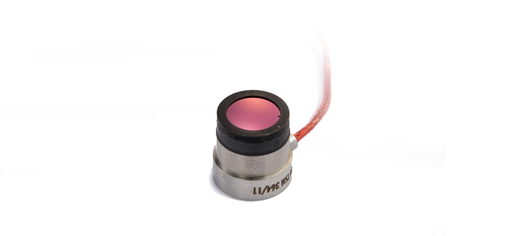
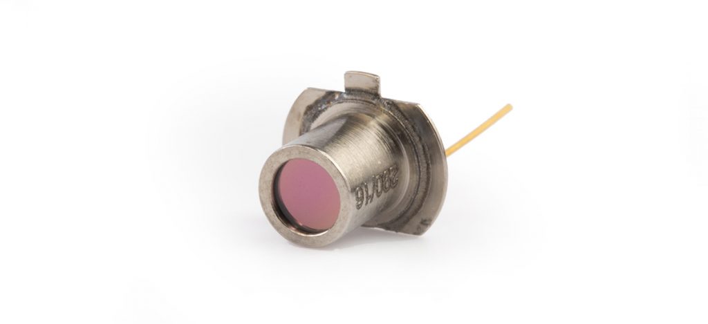
In the process of modernizing the detection systems, we have developed a method of manufacturing InSb detectors (photoresistors) cooled via liquid nitrogen. The technology involves making the InSb photosensitive element from a plate of starting material, up to a ready detector with a detection range of D* ≈ 3.7 x 10⁹ [W-1 × Hz0.5 × cm]. A very important technological activity, having a critical impact on the photoresistor parameters, is the construction of the narrowing channel (photosensitive area) – decisively influencing the photodetection parameters. The manufactured and photoelectrically tested InSb photosensitive element is mounted in a sapphire capsule, which is then equipped with a set of appropriate spectral filters and mounted in the housing. During the entire technological process of manufacturing of PbS and InSb photoresistors, we follow in-house developed inter-operational QC procedures to avoid the use of defective components in the final products.
For the production of InSb photodiodes (also intended to be used in the VSHORAD missile detection systems), it was necessary to develop our own technology of making diode photosensitive elements. On the surface of the InSb substrate, p + -n junctions were produced by ion implantation, while photolithography method was used to define the configuration of the photosensitive area as well as other specific fields, e.g., gold contacts. As a result of the technological process, the identical geometric shape of the InSb photodiode in relation to the photoresistor was obtained.
As a result of replacing the InSb PC photoresistor with the InSb PV photodiode, we obtained the following benefits:
PbS photodetector

As part of the work carried out together with the Institute of Optoelectronics of the Military University of Technology, we have developed the design and technology for manufacturing PbS (lead sulphide) photodetectors that are unique in the world. Thanks to the developed technology, we offer custom-made PbS detectors with customer-desired parameters, various structures, dimensions and shapes. The detectors meet the requirements set up for use in ammunition and rocket technology. A technology for the production of photosensitive PbS material in the form of a thick layer on a quartz substrate by the liquid phase deposition method has been developed. The obtained layers are in a monocrystalline form thanks to the use of appropriate admixtures that initiate and stabilize the deposition process. PbS plates were obtained on a quartz backing with dimensions of 25 x 25 mm, with a very homogeneous distribution of the specific resistance of the material. The obtained base material showed stable parameters in the operating temperature range -40 ° C to + 50 ° C. This form of the starting material allows for the production of PbS detectors (photoresistors) with a spectral range of 1.7-2.4 μm (mid-wave infrared – MWIR, room temp.) for the Self-Guiding Head of the VSHORAD missile, based on our own technology, with a detection level of D * ≈ 1 × 10⁹ [W-1 × Hz0.5 × cm] and allows for made-to-order PbS detectors with surface dimensions from 0.5 × 0.5 mm to 3 × 3 mm, as required by the customer. One should also mention the possibility of making these detectors in the form of photodetectors operating at room temperature, with thermoelectric cooling using high power Peletier modules or at cryogenic temperatures of liquid nitrogen. The latter takes advantage of shifting the maximum spectral sensitivity of the PbS photodetector from a wavelength of approx. 2 ÷ 2.7 μm (room temperature) to a wavelength of 3.3 ÷ 4.0 μm (liquid nitrogen temperature 77K). During the technological process of manufacturing of PbS and InSb photoresistors, we follow in-house developed inter-operational QC procedures to avoid the use of defective components in the final products.
PbSe photodetector

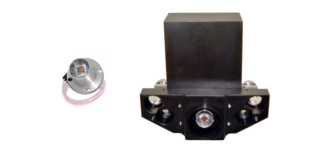
The experience gained during the development and production of infrared detectors resulted in the implementation by Telesystem-Mesko engineers of a PbSe detector (lead selenide), which was used to modernize and manufacture a detection module based on a thermoelectrically cooled PbSe photosensitive element. Together with the Institute of Optoelectronics of the Military Universiti of Technology, we have modernized the detection module for the P-22 guided anti-ship missile. In terms of modernization, the method of cooling the detector has been changed, which improved both the tactical and technical parameters of the homing warhead. This development was implemented into mass production and applied in missiles from the resources of the Polish Navy, as well as at foreign users, including Vietnam, Algeria, the USA and Japan.